How to choose a decoupling capacitor
September 27, 2026 · Updated September 30, 2026
One 100 nF ceramic at every supply pin, in an X7R or better dielectric, placed so the loop from pin to capacitor to ground plane is as small as you can draw it. Add one bulk capacitor of a few microfarads per rail per device. Placement matters more than the value.
What the capacitor is for
A logic chip does not draw a steady current. It draws a spike every time its outputs switch, and that spike rises in a nanosecond or less. The voltage regulator feeding the board cannot answer in a nanosecond, because it is metres away in electrical terms and its control loop responds in microseconds.
So the chip borrows from a capacitor sitting next to it, and the regulator refills that capacitor at its leisure. Without one, the supply pin sags on every switching edge. A supply that sags below the logic threshold gives you a chip that resets, or one that works only until the room warms up.
Why the loop beats the value
The path from the supply pin, through the capacitor, to ground and back is a loop of wire, and every loop has inductance. Inductance opposes a fast change in current, which is the one thing you need here.
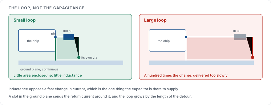
That is why a 100 nF part 2 mm from the pin outperforms a 10 µF part 20 mm away on fast edges. The larger capacitor holds a hundred times the charge and cannot deliver it quickly enough to matter.
Three things shrink the loop:
Put the capacitor on the same side of the board as the chip, beside the pin it serves.
Give it its own via to the ground plane, at the pad, instead of sharing a via down the row.
Keep the ground plane continuous underneath. A slot in the plane sends the return current around it, and the loop grows by the size of the detour.
Which dielectric
Ceramic capacitors are graded by how much capacitance they keep across temperature, and the grades are not close to each other.
| Code | Capacitance change over its range | Use for decoupling |
|---|---|---|
| C0G or NP0 | around 0.3% | Excellent, though only available in small values |
| X7R | within 15% from -55 to +125 C | The default choice |
| X5R | within 15% from -55 to +85 C | Fine for consumer temperature ranges |
| Y5V | +22% to -82% | No |
A Y5V part is sold with a headline value it holds at room temperature and loses most of in a cold car. It exists because it is cheap and small for its nominal value.
The derating nobody mentions
A class 2 ceramic also loses capacitance under DC bias, and on small packages the loss is severe. A 10 µF 0603 part rated at 6.3 V can measure a fraction of its nominal value with 5 V across it, because the same thin dielectric that makes it small is the thing that saturates.
Check the manufacturer's bias curve instead of the headline number. Where the curve is unflattering, choose a larger case size or a higher voltage rating for the same nominal value. A 25 V part at 5 V keeps far more of itself than a 6.3 V part at 5 V.
The 100 nF plus 10 nF habit
Placing a 100 nF and a 10 nF in parallel at each pin is common, and it comes from a reasonable idea: the smaller part has a higher self-resonant frequency, so it should cover the band where the larger one has turned inductive.
Between those two resonances the pair forms a parallel resonance, where the combined impedance is higher than either part alone. Whether that peak lands somewhere harmful depends on the board. Analog Devices MT-101 covers the behaviour, and the usual conclusion is to prefer several capacitors of the same value in parallel, which lowers the impedance broadly and lowers inductance by sharing the current across more loops.
What to fit, in practice
| Where | What |
|---|---|
| Every supply pin on every chip | 100 nF, X7R, smallest case you can assemble, closest possible placement |
| Each supply rail entering a device or a section | 1 to 10 µF, ceramic or tantalum, near the point of entry |
| The board's power input | Tens to hundreds of µF, electrolytic or polymer, to hold up against the supply cable's inductance |
| A chip with separate analogue and digital supply pins | Its own 100 nF per pin, and the split kept as the datasheet draws it |
Where a datasheet specifies a decoupling arrangement, follow that instead of this table, per How to read a datasheet. The manufacturer measured the part; the table is a starting point for parts whose datasheet stays quiet.
Sources
Analog Devices MT-101, Decoupling Techniques, on loop inductance, self-resonance and paralleling capacitors
IEC 60384-1, the generic specification for fixed capacitors, which defines the temperature characteristic codes
The bias and temperature curves for your exact part number, from the manufacturer, which is the only place the real capacitance appears